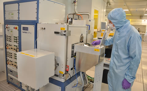
Integrated Photonics cleanroom

The integrated photonics facility is a 200m2 cleanroom designed for planar processing of a very wide range of materials not normally found in silicon processing facilities, from PTFE to germanium telluride, KY1-x-yGdxLuy(WO4)2 to Pyrex, and from ytterbium metal to lutetium biphthalocyanine. The prime purpose of this facility is to take raw and commercial materials, as well as those made by our researchers, and process them to realise photonic devices for use in applications from telecommunications to all-optical data processing and from biochemical sensing to the lab-on-a-chip. Thin film deposition, photolithography, etching and diffusion processes can all be applied to full wafers or unconventionally small or irregular samples.
Achievements
- Takes raw, novel and commercial materials and processes them to realise photonic devices for broad applications, from telecommunications to biochemical sensing, with examples including:
- CMOS-compatible supercontinuum chips produced in highly nonlinear high-k dielectric films on silicon.
- A biosensor chip which can detect and identify up to 32 trace organic pollutants simultaneously in river water at ppt levels, such as oestrone at 1ppt and bisphenol-A at 20ppt.
- The world’s first Titanium: Sapphire laser on a chip.
High-gain erbium-doped waveguide amplifiers for low-cost telecomms systems.
Facility contact
Contact us to discuss how you can access our facilities for research and development projects.
University of Southampton staff can find out how to access the facilities by visiting the Zepler Institute Sharepoint.
Equipment
Click to view the Integrated Photonics equipment list